
Illumination Economics, Not Resolution: What Ushio's LED-Equipped UX-4 Aligners Change on the Fab Floor
By Michael Torres | WorldIndustrialWeekly
Ask a power-device or MEMS production manager where the least visible cost in a lithography cell sits, and the answer is rarely the mask set or the wafer catalog. It is the lamp cabinet: pre-heat before the first exposure, cool-down between lots, a fixed replacement interval for a consumable that contains mercury, and a waste stream the site's environmental group has to document shift by shift. It is against that operating reality that Ushio Inc. has opened orders for the LED light-sourced models of its UX-4 series full-field projection aligners, UX-44101SCB and UX-45114SCB. The change is narrower than a resolution breakthrough and, for most compound-semiconductor and sensor lines, considerably more consequential: it rewrites uptime, consumable spend and chemical compliance at the same time.
Readers whose mental model of lithography is built around leading-edge scanners should note the scope. The UX-4 family addresses power semiconductors, MEMS sensors, and communication and photoelectronic fusion (optical semiconductor) devices, layers where dose, depth of focus and wafer handling, not minimum printable pitch, dominate yield and cost per die.
Why the Light Source Became the Story
Two forces converge on the illumination unit. The first is regulatory: environmental rules on chemical substance use and emissions keep tightening across the semiconductor industry, and mercury-bearing components are precisely the kind of item that plant chemistry audits linger on. The second is physical: as soon as light intensity falls short, layers that need a high exposure dose simply take longer to print, which is the remaining challenge that has slowed LED adoption in lithography equipment.
Mercury arc lamps have long been the default because they are broadband, emitting across a wide ultraviolet-to-visible band with usable peaks around the i-line, g-line and h-line regions, as surveyed in an Optics Express study of solid-state illumination for mask-aligner lithography. LEDs are narrowband by nature, so matching the effective dose delivered at the wafer plane is an optical-engineering problem rather than a drop-in substitution. Ushio's answer is an LED light source unit built from solid-state light source design technologies the company has developed since its founding, rated at intensity equivalent to conventional mercury lamps, and fitted into UX-44101SCB and UX-45114SCB. In other words, the claim under test is not "LED instead of lamp" but "LED at mercury-level dose without surrendering throughput".
Demand Signals Behind the Order Book
Next-generation electronic devices required by the evolution of IoT, 5G and mobility are pushing two contradictory demands at once: larger wafer formats and finer, more precisely registered layers. Market data makes the mix concrete rather than hypothetical. According to Mordor Intelligence's silicon carbide wafer analysis, 6-inch substrates still held 53.69% of the SiC wafer market in 2025 while 8-inch formats were expanding at a 14.91% CAGR, meaning most device makers are running a two-size inventory for years, not switching overnight. SAE's assessment of SiC and GaN power electronics puts the arithmetic on that move: going from 150 mm to 200 mm raises dies per wafer by roughly 1.8x for typical SiC devices, which is the real justification for the 6inch/8inch support on the new models.
On the packaging side, the dose-critical steps are growing fastest. Fortune Business Insights sizes the global wafer level packaging market at USD 9.94 billion in 2026, rising to USD 23.34 billion by 2034 at an 11.26% CAGR, and it is exactly the bump and WLP work described below that consumes the most exposure energy per wafer. MEMS tells a parallel story: specialty and MEMS foundry demand is reported to be accelerating at around a 12% CAGR, several times the growth of the device market itself, according to a Microsystem Engineering Conference recap published by Rogue Valley Microdevices. More layers, thicker films, bigger wafers, and more substrates that are not silicon at all.
The Data Sheet, Read as a Capacity Plan
Two details deserve attention from anyone building a capital case. First, the family is not single-irradiance: the 4inch tool is specified at 100mW/cm 2, while the 6inch/8inch models sit at 40mW/cm 2, so "equivalent to a mercury lamp" has to be evaluated layer by layer and tool by tool, not taken as one headline number. Second, the depth of focus is held constant at ±10μm across the range, which is what allows 3D surface shapes and thick-film resist exposure on both small- and large-format tools. Resolution splits as expected by format, 2μm on the smaller field and 2.8μm on the larger φ200mm exposure field, against φ100mm on the 4inch model.
| Parameter | UX-44101SCB (LED) | UX-45114SCB (LED, provisional) | UX-45114SC (lamp reference) |
|---|---|---|---|
| Wafer size | 4inch | 6inch/8inch | 6inch/8inch |
| Exposure field | φ100mm | φ200mm | φ200mm |
| Resolution | 2μm | 2.8μm | 2.8μm |
| Depth of focus | ±10μm | ±10μm | ±10μm |
| Overlay, top side | ±1.0μm | ±0.8μm | ±0.8μm |
| Overlay, back side | ±1.5μm | ±1.0μm | ±1.0μm |
| Wavelength / intensity | i Line, 100mW/cm 2 | i Line, 40mW/cm 2 | i Line, 40mW/cm 2 |
| Substrates | Si, GaAs, GaN, GaP, InP, SiC, Glass, Sapphire, Ceramics, LN, LT, Thin & Thick | ||
| Automation options | EFEM, automatic mask handling, SECS/GEM online, AGV, inline with coater/developer | ||
*Appearance and specifications are subject to change without prior notice.
Capabilities that carry over unchanged
- Full-field projection exposure keeps the reticle out of contact with the wafer, avoiding mask damage while delivering high productivity of 120 WPH or more
- Deep depth of focus supports conformal patterning over topography, including 3D surface shapes and thick-film resists used in MEMS and power packaging
- Inline, Online and OHT/AGV integration options let the tool enter an automated fab layout rather than a stand-alone bench
- Mercury-free operation is available with the LED light source, removing the lamp from the hazardous-materials inventory
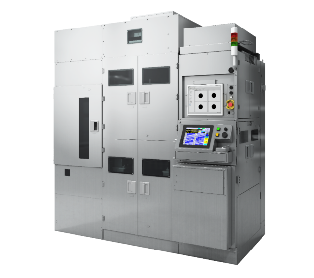
Tool appearance
What Changes After Installation
Compared with conventional mercury lamps, the equipment supports instantaneous turn-on and turn-off during exposure. That single behavioural difference reshapes three budget lines. Idle time between lots no longer burns lamp hours; the source lifetime, no longer degraded by thermal cycling, stretches out; and the running cost after installation falls, with the spent-lamp disposal question removed for the LED configuration. Facility teams have been moving in this direction anyway: the University of Waterloo's quantum nanofabrication facility, for example, describes UV-LED sources as an attractive alternative to hazardous, energy-consuming mercury lamps when its aligners were upgraded.
Performance is the other half of the equation. With the new equipment, even high-exposure-dose processes such as Bump and WLP can reach high throughput equivalent to conventional mercury lamp equipment, which is the point that converts an environmental preference into a manufacturing business case. As a leading company in full-field projection aligners for wafers, Ushio positions the release as an extension of a series with a long installation record in improving production efficiency.
Common Misconceptions Worth Retiring
- "LED parity means the swap is transparent for every layer." Parity is claimed at the source, not at the printed feature. Dose-to-clear, film thickness and standing-wave behaviour still have to be requalified on the highest-dose layers, and the two LED models ship at different irradiance levels.
- "Mercury lamp phase-outs are already mandated for lithography." The Minamata Convention's agreed phase-out dates cover mercury-added products and, per UNEP's guidance, target lamps for general lighting such as fluorescents by 2027. Lithography illumination is being displaced mainly by fab-level chemical-use rules, energy and consumable economics, not by that clause; buying teams should not assume a compliance deadline forces the decision.
- "Bigger wafers make legacy formats obsolete." The tool family itself is the counter-evidence: 4inch remains specified alongside 6inch/8inch, and compound-semiconductor, filter and photonics lines on sapphire, ceramics, LN and LT substrates are long-lived.
- "Throughput figures are interchangeable between sources." The 120 WPH or more rating reflects full-field projection productivity, not a single recipe. Real output on thick-resist or bump layers depends on dose, and the back-side overlay budget matters more than the front side on flip-chip work.
Action Plan for Equipment and Process Owners
- Map your dose-critical layers first, bump, WLP, thick resist and high-aspect MEMS vias, and record dose-to-clear plus measured film thickness for each before any source comparison.
- Request irradiance, uniformity and spectral-peak data per model rather than per series; treat the 40mW/cm 2 large-wafer configuration and the 100mW/cm 2 small-field configuration as separate process windows.
- Qualify against topography, not flat test wafers: verify the ±10μm depth-of-focus budget on patterned substrates and confirm top-side and back-side registration at ±1.0μm and ±1.5μm, or ±0.8μm and ±1.0μm on the larger-format models.
- Check automation readiness early, EFEM, mask handling, SECS/GEM messaging, AGV handoff and coater/developer inline, because integration effort typically overshadows the difference between illumination technologies.
- Rebuild the consumable model: quantify lamp purchase frequency, warm-up and cool-down losses, mercury waste handling and disposal, then compare against LED source maintenance over the planned tool life.
- Run a substrate-mix pilot spanning SiC, GaN and sapphire lots if your fab is migrating wafer sizes, since 6-inch and 8-inch production will coexist for several years.
- For the newest large-wafer configuration, treat specifications as provisional and lock deliverables and test-method agreements into the purchase order before volume ramp.
FAQ
Is the LED source genuinely comparable to a mercury lamp?
Ushio Inc. states that the LED light source unit reaches intensity equivalent to conventional mercury lamps, and that high-dose Bump and WLP processes reach throughput equivalent to lamp-based equipment. Independent confirmation still requires on-tool dose and critical-dimension data for your specific resist stack.
Which applications gain the most?
Power semiconductors, MEMS sensors, and communication and photoelectronic fusion devices, especially where thick resists, topographical surfaces and high-dose metal or solder processes are routine.
Can it pattern over non-planar wafers?
Yes. The deep depth of focus of ±10μm is the enabling specification for 3D surface shapes and thick-film resist exposure.
What about mercury regulation and disposal?
The LED configuration removes mercury from the exposure optics, eliminating associated disposal handling. General-lighting phase-out rules under the Minamata Convention do not themselves cover litho lamps, so the case rests on site chemistry policy and operating cost.
How does the series fit existing fab automation?
Automation compatibility covers Inline, Online and OHT/AGV arrangements, with EFEM, automatic mask handling and SECS/GEM online support listed in the specification table.
Terminology
※1 Bump: a process to form microscopic bump-shaped metal terminals called bumps (such as solder balls) on the electrode parts of semiconductor chips.
※2 WLP: a process to perform batch packaging (encapsulation) and terminal formation on the whole wafer before cutting the silicon wafer into square chips.
Outlook
Order intake for the LED-equipped models runs from July 2026, according to Ushio's own announcement, which gives fabs one budget cycle to convert the argument into a plan. The likely pattern is replacement-driven rather than greenfield: source-level changes are easiest to justify when an existing mercury-lamp aligner is being retired or a line is being consolidated onto larger substrates. The wider signal for industrial buyers is that lithography competition in mature-device segments is shifting from resolution alone to total cost of ownership, chemical footprint and integration readiness. Ushio's pitch, that a solid-state source can hold dose and throughput while removing a hazardous consumable, will be judged on installed lines rather than spec sheets, and the next twelve months of order conversion in power and MEMS fabs is the yardstick to watch.
Have a tip on industrial lithography or fab equipment strategy? Reach the WorldIndustrialWeekly editorial desk at news@industrialweekly.com.