
Taylor Fab 2 Is Booked Before Its First Wafer: Reading Samsung's AMD HBM Base-Die Order as an Industrial Signal
By Michael Torres — WorldIndustrialWeekly
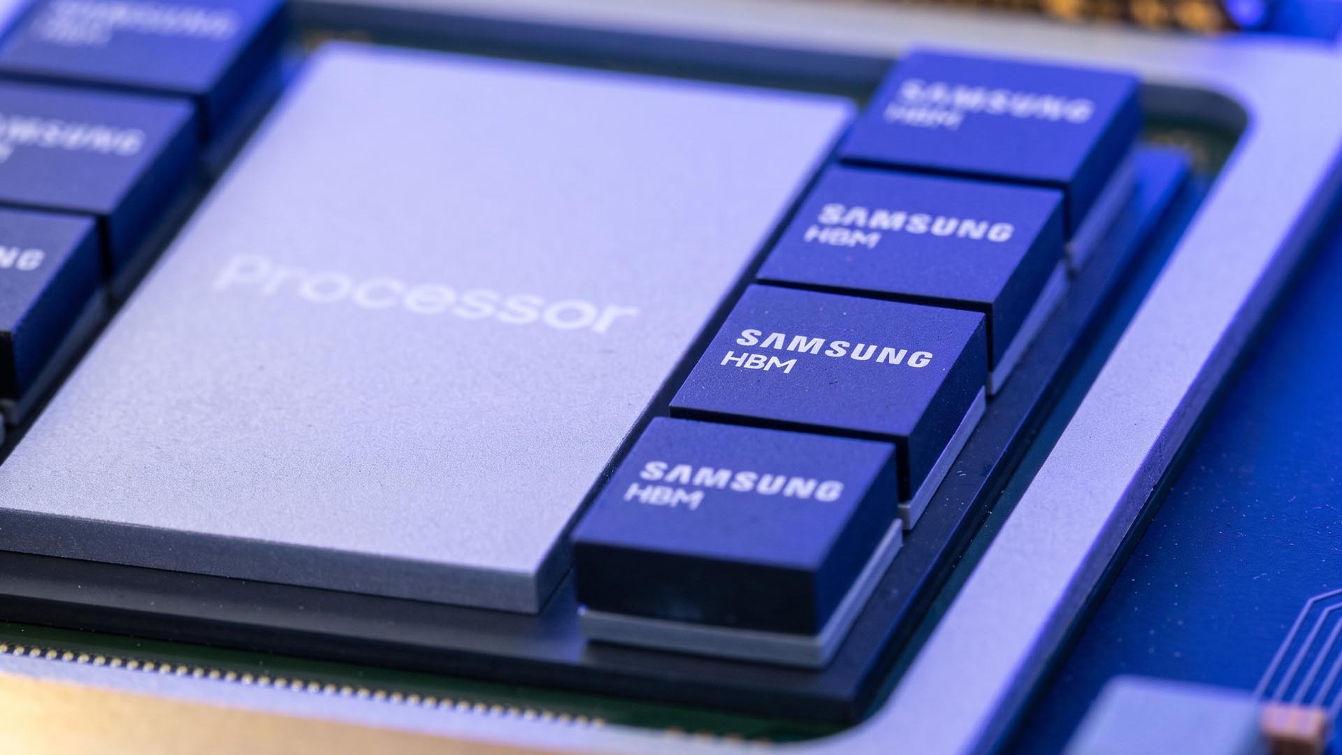
A plant that will not ship a commercial wafer until 2030 has already been allocated. That sequencing — capacity committed years ahead of silicon — is the real story for operations managers, procurement leads and capital planners, and it says less about one contract than about how the AI hardware supply chain is now being reserved: forward, by the wafer, and across borders. The trigger is the National Business Daily report of November 3 stating that Samsung's foundry business has secured the base-die order for AMD's next-generation high bandwidth memory, with output earmarked for the planned second Taylor wafer fab (Taylor Fab 2) in Texas — and with the site's planned capacity nearly full, AMD taking most of it.
What the Reporting Actually Says
Restating the verified core, because the surrounding commentary tends to drift: Samsung Electronics reportedly won the base-die order for AMD's next-generation high bandwidth memory, and Samsung foundry output for it is planned at the second Taylor fab in Texas — the same Taylor Fab 2 site on the De克萨斯州 industrial corridor. Those base dies would then travel back to South Korea for stacking and advanced packaging with DRAM produced at Samsung's home memory plants. The reported construction schedule is unchanged: site preparation complete, main works beginning November 2026, equipment installation from February 2029, commercial high-volume output in 2030. The plant footprint is described as roughly 2.7 million square feet, about 1.5 times the size of the first Taylor fab, and the technology target is 2 nm processes and beyond, matching what next-generation HBM base dies demand on power and performance.
Why a Base Die Turned a Memory Component Into a Foundry Product
For years HBM was read as a DRAM story: more layers, faster pins, better yields. The base die changed that equation. Sitting at the bottom of the stack, it handles internal data routing, control logic, repair and interface functions, and under the HBM4 generation it stops being a simple glue chip. JEDEC's HBM4 specification widens the interface from 1,024 bits to 2,048 bits per stack and sets baseline pin speeds around 8 Gb/s, giving roughly 2 TB/s per stack — figures summarized in design guides from Siemens EDA and in JEDEC coverage across the trade press. That is why the base die is a logic chip, why it requires advanced logic process technology, and why foundries now contest a category that used to belong to memory makers alone.
The direction of travel matters for anyone specifying memory into 2027–2029 product roadmaps. HBM4E is expected to push pin rates into the 12–12.8 GT/s range, lifting per-stack bandwidth toward 3–3.3 TB/s according to Tom's Hardware's reporting of the JEDEC timeline, while the newer SPHBM4 profile narrows the interface to 512 bits so that cheaper organic substrates can replace expensive silicon interposers. In practice, the base die is becoming the place where customers insert proprietary logic — which makes it strategically sticky and a very different procurement object than commodity DRAM.
Case Study in Sequencing: How the First Taylor Fab Got to Full Booking
Read the AMD story against the ramp of the first Taylor fab, and the industrial logic becomes clearer. That plant's lead products are automotive and edge AI logic — Tesla has been reported as its anchor customer, with industry reporting in September 2026 describing trial 2 nm wafer starts and advanced-node capacity already committed ahead of volume production. The scale of state support behind the site is public record: under the CHIPS and Science Act the U.S. Department of Commerce committed up to $4.745 billion in direct funding to Samsung, disclosed in December 2024 as support for a Texas complex covering two advanced logic fabs and an R&D fab in Taylor plus expansion in Austin, part of an investment program Samsung has described in the tens of billions of dollars.
Capex data from SEMI places that single decision in a system context. SEMI's 300 mm Fab Outlook, presented at SEMICON West in October 2026, forecasts global front-end 300 mm equipment spending of $149 billion in 2026, up 31% year on year, rising to about $227 billion by 2029; Americas investment is projected to more than double from $18.1 billion in 2026 to $40.6 billion in 2029, with 13 new 300 mm fabs or lines starting up or shipping first silicon in 2026 and 23 in 2027, including three U.S. starts in 2026 and four in 2027. A second Taylor plant booked before construction begins is not an anomaly in this dataset — it is the pattern.
The Demand Backdrop: Rationing on Both Sides of the Stack
TrendForce's memory research gives the quantitative edge to the argument. HBM together with RDIMM is expected to account for about 51% of DRAM bit supply in 2026 (TrendForce, August 2026), and the firm has signalled that HBM stays supply-constrained into 2027, with 2027 allocation negotiations handing suppliers pricing leverage. On the logic side, the same research house recorded global top-10 foundry revenue near $53.49 billion in 2Q26 and noted SMIC narrowing the share gap with Samsung — a reminder that the foundry unit is simultaneously defending logic share and trying to monetize a rare hybrid opportunity in memory-adjacent silicon.
Over the past several years, Samsung's advanced logic business has struggled to win the same level of customer recognition as TSMC in high-performance computing and AI chips. This base-die order is the clearest attempt yet to convert its memory strength and advanced logic process capability into a single offer inside the AI hardware chain.
For industrial buyers the implication is uncomfortable and concrete: competition for capacity is no longer GPU versus GPU, but GPU, accelerator, DRAM bits and the base dies that stitch them together — all drawing on a finite pool of advanced wafer starts and packaging slots.
The Nvidia Constraint: Standardization as an Entry Barrier
The reporting also flags a structural obstacle. Nvidia has been described as wanting its memory suppliers — Samsung, SK hynix and Micron — to standardize the base die for next-generation customized HBM on TSMC process, so that parts from different vendors behave identically. The reasoning is qualification arithmetic: foundries differ in process, power envelope and thermal behavior, and if each supplier's base die comes from a different fab, an accelerator program accumulates characterization and compatibility work it never budgeted for. Common manufacturing reduces variance between suppliers and lowers the difficulty of developing next-generation customized HBM.
That is why a win at AMD does not automatically translate into an equivalent position in Nvidia's customized HBM chain. Samsung is still testing and qualifying its advanced wafer fabrication processes against those requirements. The realistic opening is volumetric: if future Nvidia demand exceeds the capacity TSMC can supply, incremental orders have somewhere to go. Qualification, not capacity, is the gate.
Three Misconceptions Worth Correcting
- Booked capacity equals delivered capacity. A plant that begins moving in tools in February 2029 and ramps in 2030 can still slip on tool delivery, yield learning or permitting. Reservations this early are normally contingent, not contractual.
- HBM is a memory product, so only memory makers matter. Unlike conventional DRAM, an HBM base die is a logic chip carrying complex control functions, so the chain now needs a foundry, a DRAM fab and an advanced packaging line to align on one schedule.
- U.S. fabs mean U.S. supply chains. Under the plan Samsung is reported to pursue, wafers made in Texas cross the Pacific for stacking in South Korea. Localizing the front end does not localize the back end.
Risk Register: Where the Plan Can Still Break
First, the trans-Pacific round trip. Base dies fabricated in Texas and stacked in South Korea add ocean freight, customs handling and inventory buffering into a component that sits on the critical path of accelerator programs. Any packaging or test constraint on the Korean side converts directly into schedule risk for the American customer. Advanced packaging is already the industry's acknowledged chokepoint, a point made in CSIS's analysis of the Texas semiconductor ecosystem and echoed across trade coverage of assembly, test and packaging capacity.
Second, site-level industrial constraints. CSIS and local Texas reporting repeatedly identify water demand, grid connection timelines and the shortage of skilled construction and process engineers as the binding constraints on Central Texas fabs — not capital availability. A facility of 2.7 million square feet is, operationally, a civil infrastructure project before it is a semiconductor project.
Third, the confirmation boundary. The AMD order and the customer split come from Korean media citing industry sources, and Samsung has said only that it cannot confirm client-related information. AMD's order scale, and whether Nvidia procurement is settled at all, should still be treated as media reporting rather than officially published contract details.
Action Guidance for Manufacturers and Procurement Teams
- Re-baseline memory assumptions for 2029–2030 designs. If a roadmap depends on HBM4-class bandwidth, treat base-die sourcing and its fab location as a named dependency, not a supplier detail.
- Diversify on process, not only on vendor. Three suppliers stacking on one foundry node is still a single point of failure; ask which fab and which node each stack's base die uses.
- Model the logistics leg explicitly. Add round-trip transit and customs buffer to any architecture that pairs U.S. wafer fabrication with overseas stacking.
- Watch equipment milestones, not announcements. Tool installation beginning February 2029 is the first hard signal that a 2030 ramp is real.
- Treat packaging capacity as a leading indicator. Where stacking and test capacity sits is where HBM availability will be decided.
FAQ
What exactly did Samsung reportedly win?
According to the National Business Daily report of November 3, a foundry order for AMD's next-generation HBM base die, to be produced at the planned second Taylor fab in Texas, with that plant's planned capacity nearly fully booked and AMD holding most of it.
Why would an accelerator maker care where a base die is fabbed?
Because the base die's design and manufacturing process directly affect memory bandwidth, power consumption and overall performance, and mixed sourcing forces extra validation across otherwise interchangeable memory suppliers.
When could this capacity actually reach production?
The reported schedule puts main construction from November 2026, equipment installation from February 2029 and commercial mass production in 2030.
Is the order confirmed by the companies involved?
No. Samsung has stated it cannot confirm client information, so customer names and capacity allocation remain media reporting.
Where the Competition Moves Next
If the plan is ultimately realized, Samsung would have, around 2030, a large advanced-process plant aimed squarely at next-generation HBM base dies, feeding its own memory lines — a vertical seam that neither a pure foundry nor a pure DRAM maker can easily replicate. The broader read for industrial management is that rivalry in the AI chip chain is no longer limited to GPUs and DRAM themselves; the base die and the process that manufactures it have become a contested battleground among semiconductor giants. The scarce asset is not design capability alone, but aligned wafer, packaging and logistics capacity, reserved years ahead. Teams that keep treating memory as a commodity line item will find it behaving like allocated capacity: expensive, booked early and geographically complicated.