
From Lab Promise to Purchasing Decision: What Industrial Buyers Should Ask About Optical Interconnects Now
This week’s $115 billion Marvell-Lumentum deal settles the question most industrial technology teams have been circling: silicon photonics is no longer insurance against copper’s power limits, it is a line item. Read plainly, the state of play today is that optics is deployable for scale-out fabrics and network reconfiguration now, while most chip-to-chip links inside the rack stay copper until volume photonic capacity ramps; several suppliers point to 2027 as the turn.
What actually changed in this cycle?
Answer first: capital and manufacturability moved, the physics did not. The engineering case for optics has been stable for years. What is new is that strategists now price photonics as a market to be captured rather than a technology to be proven.
Just two years ago, a workshop panel at the OFC conference in San Diego asked whether AI would become the killer application for silicon photonics. At that time, the panel report captured the mood precisely: "It was clear from the presentations that we are at a potential turning point for silicon photonics. But there were still challenges in terms of scaling, energy efficiency, packaging, ecosystem, and tools like EDA and third-party IP, as well as materials."
Read that list again against purchase orders being written now: scaling, packaging and ecosystem are no longer open research questions, they are supply constraints — wafer slots, photonic test coverage, fiber-array units, assembly yield. That reframing is the most useful signal the Marvell-Lumentum number sends to an industrial reader, because constraints can be planned around in a way that unsolved physics cannot.
Who is betting on optical circuit switching, and why does the factory plan matter more than the demo?
Short answer: a switch that cannot be fabbed at volume is a lab result, not a product. That is the dividing line inside the current optical circuit switching (OCS) cohort.
Salience Labs has raised $125 million in Series B funding to accelerate deployment of its OCS technology. Its backers include Applied Ventures, AMD Ventures and Intel Capital — three corporate investors whose portfolios map onto the compute, accelerator and foundry layers the company must ultimately sell into.
In an interview, Salience Labs CEO and co-founder Vaysh Kewada explained why she believes this is the right moment for optical switching, and how the company plans to reach volume manufacturing and commercial adoption. Her account rests on two decisions that matter more to buyers than any bandwidth headline: the architecture is deliberately built on foundry processes able to support volume production, and the team aligned with co-packaged optics (CPO) manufacturing strategies early on. She also pointed to 2027 as a critical inflection year for volume production and deployment of the company’s OCS technology.
In remarks to EE Times, Kewada said: "We’ve taken the approach of developing out an optical circuit switch that’s optical end-to-end so we’re never transforming the payload or the data into the electrical domain. The second differentiating standpoint is that we’ve chosen to take a fully integrated on-chip approach. And we’ve overcome the loss aspect of integrating optics onto the chip through the development of our own amplifiers that are also integrated on chip."
Translate that into floor terms. Keeping the payload out of the electrical domain removes optical-electrical-optical conversion, which is where serialization and retiming power accumulates across a fabric. On-chip amplification attacks insertion loss — historically the reason integrated optics stopped at short reaches. This context also helps explain why Marvell is interested in bringing Momentum into its already strong connectivity portfolio: the acquirer is assembling a laser-and-loss budget, not collecting SKUs.
Is there a second architecture in the race, and what does that change for procurement?
Yes. In the same week that Salience Labs announced its funding round, Voyant Photonics, another startup competing in the OCS space, said it is developing a chip-scale OCS engine for AI data center networks, intending to offer customers a compact optical switching building block that can be integrated into next-generation data center switching platforms.
Voyant is not starting from scratch: it has already developed a high-density silicon photonics switch matrix that routes light for its FMCW LiDAR systems. Instead of moving mirrors or continuous analog beam steering, the architecture uses discrete, solid-state optical paths. The company said this technology is now being adapted because a data center OCS implementation uses the same fundamental architecture, which can be configured to route optical signals among communication ports. Voyant plans to offer its OCS technology as an engine that optical networking companies can incorporate into their own platforms.
For operations teams, engine-style business models open a diligence gap: the switch you rack may carry somebody else’s photonics. Three questions close it — who owns the photonic integrated circuit, who wafer-tests it, and who carries the replacement obligation when a lane degrades.
How fast is the scramble for control points?
Faster than a typical component cycle, and it is being measured in access to scarce layers rather than in revenue. A report published last month by Woodside Capital Partners, titled "The Interconnect Imperative—Why AI Is Forcing the Semiconductor Industry to Go Global", stated: "In the space of fifteen months, Marvell paid $3.54 billion for Celestial AI; Nvidia put $2 billion each into Coherent and Lumentum—and then $3.2 billion more into Corning; Ayar Labs closed a $650 million Series E at a $5.0 billion valuation; and Credo, Molex, GlobalFoundries, Ciena, AMD, and FormFactor each bought their way into a different layer of the stack."
The same report added: "Our view is that this is a land grab for control points—lasers, optical engines, chiplets, packaging, test, and foundry capacity—and that it will not run forever. Each deal removes a control point from the board and raises the scarcity premium on what remains; but as the gaps fill, urgency will decline. For founders, the window for premium strategic exits is open now. For acquirers, the cost of waiting is compounding."
Over the past year, the industry has moved very quickly from viewing integrated silicon photonics as an emerging alternative to copper to recognizing optical interconnects as a viable physical backbone for scaling next-generation AI infrastructure. As Woodside Capital notes, the surge in investment activity — high-ticket funding rounds or outright acquisitions — highlights a shift in which foundry economics now favor high-volume manufacturability and scaling.
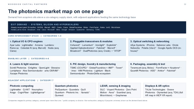
Woodside Capital Partners’ photonics market map places acquirer demand from systems, silicon and hyperscaler companies above a six-category supply stack of core interconnect and enabling technologies, while adjacent applications draw on the same technology base. It maps companies to their primary category, marks public companies or divisions with an asterisk, and is non-exhaustive. Image courtesy of Woodside Capital Partners.
Independent manufacturing news backs the foundry-economics argument. TSMC’s COUPE photonics engine was mapped from small-form-factor pluggable qualification in 2025 to CoWoS-based co-packaged optics in 2026, according to TrendForce reporting in April 2026, and coverage of SEMICON Taiwan in August 2026 described COUPE entering mass production, alongside UMC’s first mass-produced silicon photonics wafers at its Singapore fab with Silith Technology and Hon Hai’s plan to begin CPO switch shipments in the third quarter of 2026. Those are factory facts, not demo slides — and they identify the three bottlenecks buyers will actually be quoted on: wafer test, fiber array units and high-speed optical assembly.
Where does copper still win, and where does it stop?
Answer: copper still wins on reach economics and replaceability inside the rack. It stops winning the moment the signal has to cross a row, a pod or a building, or the moment the electrical path needs re-timing.
The decision variable is energy per bit. Analyst work on co-packaged optics places traditional copper cables driven by linear SerDes at 224G near 5 pJ/bit (SemiAnalysis, 2026), while a 2025 arXiv study of 3D-integrated optics argues that at about 5 pJ/bit optics is effectively at parity with passive copper and models 14.4 Tb/s of scale-up bandwidth at roughly 72 W of interconnect power. Retimed long-reach electrical links are commonly placed in the 10-15 pJ/bit band in OIF-era roadmap discussions. The practical rule for a designer: optics pays back where the electrical channel would otherwise need DSP re-timing or a second conversion stage.
The strongest production evidence for the all-optical path is not a startup demo. Google’s Jupiter fabric, described in its SIGCOMM 2022 paper and engineering blog, reported about 30% higher throughput, 40% less power, 30% lower cost and 10% faster flow completion after inserting high-radix OCS into the network spine. Google Cloud’s TPU architecture documentation extends the same logic to accelerators: reconfigurable optical circuit switches build the 3D-torus interconnect, and ICI resiliency routes traffic around failed optical links and switches. Any maintenance engineer will recognize that behavior as bypass-and-repair rather than truck-roll — which is why OCS is being adopted first for reconfiguration and availability, not for raw bandwidth.
How large is the spend, and how should operators budget it?
Treating photonics as a budget line means triangulating forecasts that are not yet reconciled. Three current estimates frame the range:
| Scope | Base | Forecast | CAGR | Source |
|---|---|---|---|---|
| Optical interconnects, total market | US$17.1 Bn (2026) | US$38.5 Bn (2033) | 12.3% | Persistence Market Research |
| Optical interconnect market | USD 18.83 Bn (2026) | USD 33.28 Bn (2031) | 12.06% | Mordor Intelligence |
| On-chip optical interconnect subset | USD 232.8 M (2024) | USD 771.4 M (2030) | 22.1% | Next Move Strategy Consulting |
Read the gap, not the headline: the aggregate layer compounds near 12% while the on-chip subset compounds above 20%. Most committed spend still sits in modules and transceivers; the fastest growth sits where optics meets the package. That asymmetry is a planning signal — forecast bandwidth and package-level exposure rather than trusting any single supplier roadmap, and keep multi-year supply commitments short enough to reprice as the acquisition map fills in.
What should you ask suppliers before signing?
- Which process and which fab? Volume claims should name a foundry photonics process and a test flow, not a device benchmark.
- What is the loss and amplifier budget? Ask for insertion loss per hop with aging margin, and whether amplification is on-chip or external.
- Is the laser field-replaceable? Externally sourced lasers and OIF ELSFP-style modules change the unit of repair; the OIF has been pushing co-packaging and external-laser interoperability work through 2026, including live multi-vendor demonstrations scheduled around ECOC 2026.
- What is the unit of replacement? A pluggable is a two-minute swap; a fused optical engine can make the line card or the whole sled the spare part.
- What port headroom do you recommend? Operators of optical fabrics commonly overbuild ports by roughly 5-10% and hold hot spares so a dead lane is routed around.
- What radix, and what does that do to my topology? High-radix OCS platforms on the market reach several hundred ports per device — Molex, for example, lists a platform supporting up to 544 ports — which flattens the fabric and cuts the electronics in the path.
- Who owns the silicon photonics IP and the second source? Engine-style supply means the switch vendor may not control the photonic die.
- What does the reference deployment prove? Ask for energy per bit at the link rate you will actually run, and for availability data over a training job, not a port.
What are the most common misconceptions?
- "Optics replaces copper everywhere." It replaces re-timed long-reach electrical links first; short-reach in-rack copper remains cheaper and more serviceable.
- "Big deals validate products." They validate control points — lasers, engines, chiplets, packaging, test and foundry capacity. A purchase order is still owed.
- "Co-packaged optics kills the pluggable." Roadmaps and standards work treat the two as coexisting tiers; front-pluggable, near-package and co-packaged variants are all in production planning.
- "Energy per bit decides the architecture." Energy per bit sets the capex line; serviceability, blast radius and spares stocking set the availability line.
- "A 2027 volume target is a schedule." It is a stated intention that depends on wafer test and packaging capacity the whole industry is competing for.
What should managers do in the next two quarters?
- Facility and operations leads: model interconnect power as its own line against rack-level budget, and rewrite spares policy for optical fabrics before the first CPO switch arrives.
- Network and platform engineers: pilot OCS where reconfiguration value is proven — topology slicing, fault bypass, capacity pooling — rather than in the shortest links.
- Procurement: require named process nodes, test coverage and laser replaceability in RFPs; treat exclusivity clauses on photonics as a capacity risk.
- Executives and investors: price the land grab as finite; the window that makes premium exits possible now also raises the cost of waiting for late buyers.
- Policy and regional planners: track where photonic wafer and packaging capacity is being sited, since that is where interconnect cost curves will be set for the next decade.
FAQ: the short answers
Are optical interconnects replacing copper now?
Partially. Optics is winning scale-out and reconfiguration roles where electrical retiming dominates power; in-rack short reach largely stays copper until co-packaged and near-package optics ramp at volume.
What is optical circuit switching in one sentence?
A switch that redirects light from one fiber to another without converting the payload into electrical signals, so bandwidth costs power and latency almost nothing at the switching point.
Why does everyone cite 2027?
Because that is when several suppliers, including Salience Labs, expect volume production and deployment of optical switching to converge with co-packaged manufacturing capacity. Treat it as a capacity forecast, not a product launch date.
Does a co-packaged design increase my outage risk?
It changes the failure domain. Reporting on hyperscale deployments suggests fused optics removes the pluggable connector as a common failure source, but when an engine fails the repair unit becomes a line card or sled — hence port overbuild and hot spares.
Is the M&A wave a buying signal or a warning?
Both. It confirms the interconnect layer is strategic, and it means fewer independent control points remain to negotiate against. Locking specifications early is cheaper; locking suppliers for long is riskier.
Sources and further reading
- Google Cloud blog, "The evolution of Google’s Jupiter data center network" (with the SIGCOMM 2022 Jupiter Evolving paper): https://cloud.google.com/blog/topics/systems/the-evolution-of-googles-jupiter-data-center-network
- Google Cloud, TPU system architecture (OCS topology, ICI resiliency): https://docs.cloud.google.com/tpu/docs/system-architecture-tpu-vm
- "Jupiter Evolving: Transforming Google’s Datacenter Network via Optical Switches", SIGCOMM 2022 (paper copy): https://web.stanford.edu/class/cs244/papers/poutievski-sigcomm22.pdf
- TrendForce on TSMC COUPE and the 2026 silicon photonics race: https://www.trendforce.com/news/2026/04/01/news-silicon-photonics-race-intensifies-as-tsmc-targets-2026-coupe-production-samsung-eyes-2029-cpo-turnkey/
- OIF, AI-era interoperability demonstrations and ELSFP co-packaging work: https://www.oiforum.com/oif-validates-ai-era-interoperability-live-at-ecoc-2026-through-multi-vendor-demonstrations-and-expert-sessions/
- SemiAnalysis, Co-Packaged Optics book (copper and optics energy per bit): https://newsletter.semianalysis.com/p/co-packaged-optics-cpo-book-scaling
- arXiv, "Accelerating Frontier MoE Training with 3D Integrated Optics": https://arxiv.org/html/2510.15893v1
- Persistence Market Research, Optical Interconnects Market: https://www.persistencemarketresearch.com/market-research/optical-interconnects-market.asp
- Mordor Intelligence, Optical Interconnect Market: https://www.mordorintelligence.com/industry-reports/optical-interconnect-market
- Next Move Strategy Consulting, On-Chip Optical Interconnect Market: https://www.nextmsc.com/report/on-chip-optical-interconnect-market-se3674
- Molex, high-radix optical circuit switch platform: https://www.molex.com/en-us/products/optical-solutions/optical-circuit-switch
Reported and edited by Michael Torres for WorldIndustrialWeekly. For corrections, data requests or to share your own optical interconnect deployment results, reach the newsdesk at news@industrialweekly.com.