
WorldIndustrialWeekly General Coverage: NVIDIA Turns Rubin Planning Toward Yield, Cooling and 8-Layer HBM4
For the next generation of NVIDIA AI compute platforms, the more urgent question is no longer only how tall a memory stack can be built. Reports place NVIDIA in discussions with Samsung and SK hynix during Q3 2026 about future products adopting more 8-layer HBM4 configurations. The Rubin series had been widely linked to 12-layer HBM4 or HBM4E, but manufacturing, cooling and supply realities are now shaping the roadmap.
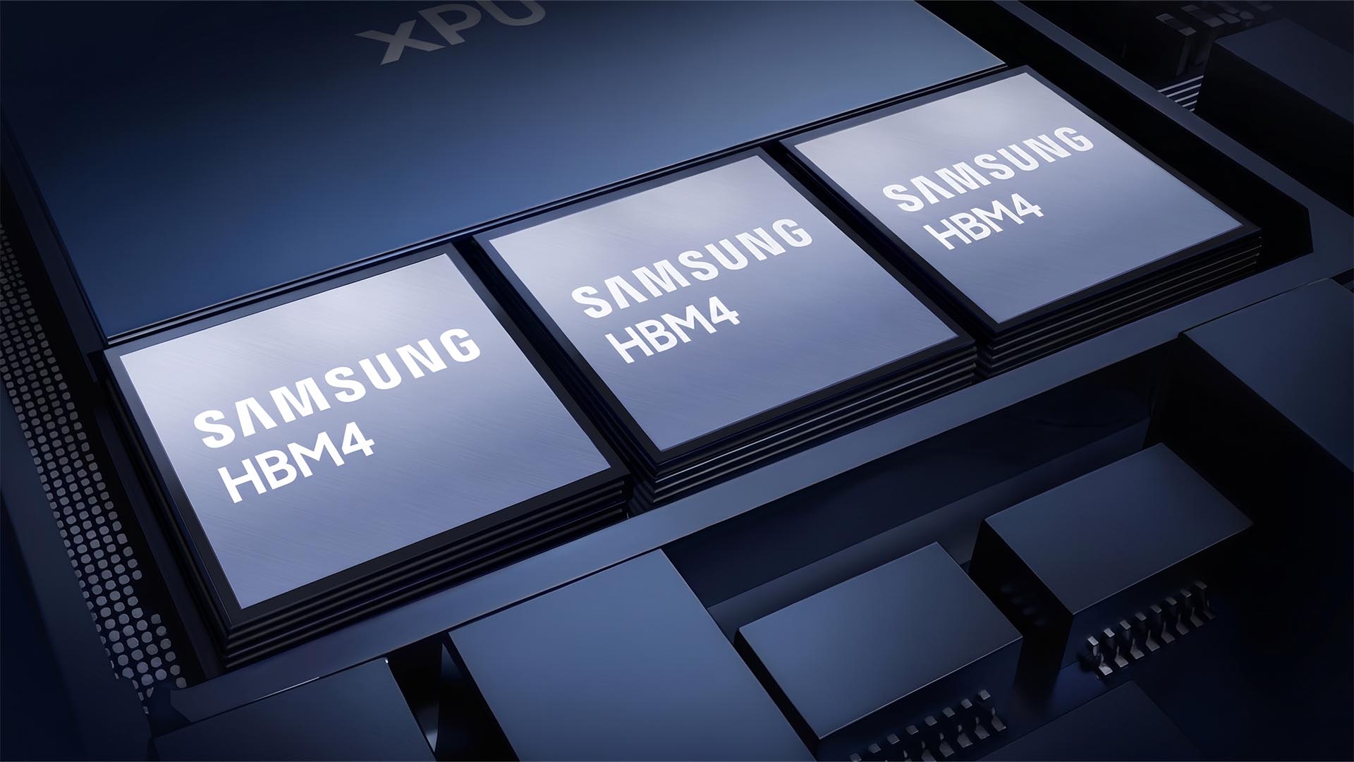
Case signal: Rubin Ultra simplifies as memory choices tighten
The clearest case for the shift is Rubin Ultra. Earlier expectations pointed to a more aggressive, larger-scale chiplet direction, but supply-chain pressure led NVIDIA to shrink parts of that plan. Reports say the product moved from a more complex scheme toward a dual-chip design, a step intended to reduce manufacturing risk and protect volume progress. In parallel, the memory decision is widening: NVIDIA is not only evaluating 8-layer HBM4, but also 8-layer HBM4E. The choice for Rubin Ultra and the NVL rack-scale system will be judged against design needs, supply capability and overall cost structure.
Why each additional layer changes yield
Industry analyses frame the trade-off as a process problem, not a performance problem. In DRAM stacking, each additional layer raises thermal resistance, makes heat removal harder, increases the likelihood of wafer-bonding defects and reduces overall yield. That is why 8-layer stacking can be read as a compromise: it gives up some capacity in a single stack, but it is easier to produce and easier to cool. The result is a configuration that balances cost, output and stability more tightly than a taller stack would.
What the cited numbers indicate
| Data point | Reported meaning |
|---|---|
| Q3 2026 | Period when NVIDIA and suppliers were reported to be discussing more 8-layer HBM4 use. |
| mid-2027 | Timing from which 8-layer versions are expected to raise their market share significantly. |
| 2027 | Target year for Rubin and Rubin Ultra as the flagship platforms succeeding the Blackwell series. |
| 12 layers and 8 layers | Current stack-count axis: a partial shift toward more 8 layers does not remove 12-layer HBM4 products. |
12-layer HBM4 products remain in the mix
This is not an exit story for 12-layer HBM4 products. Samsung and SK hynix are already in mass production with them, and they are reported to have obtained NVIDIA certification. Over the next few years, 12-layer HBM4 is still expected to remain a major part of the high-end HBM market. The expected change is in weighting: from mid-2027, 8-layer versions are forecast to take a significantly larger share.
Certification work in South Korea
Disclosures in South Korea point to the procedural side of the transition. Samsung and SK hynix are said to be preparing the components, materials and quality-validation steps needed for independent certification of 8-layer HBM4. Because the 8-layer option is less technically complex than the 12-layer option, industry sources consider the follow-on certification less likely to produce a major delay.
Common misconceptions
- "A move to 8 layers is a downgrade." The reported motivation is manufacturability: cooling, bonding yield and supply stability, not a simple performance reversal.
- "12-layer HBM4 will disappear." It will not. Certified 12-layer HBM4 products are in mass production and still matter to high-end HBM demand.
- "HBM4E is being replaced by older HBM4." No. 8-layer HBM4E is also under evaluation, so the change is about stack count and process risk, not abandonment of the HBM4 family.
Action recommendations for production and engineering teams
- Treat memory stack counts as risk indicators. For Rubin-series planning, 8-layer HBM4, 12-layer HBM4, 8-layer HBM4E and certification status should be mapped to yield, thermal design and delivery exposure.
- Connect component choices to system cost. NVL rack-scale system design decisions are expected to weigh overall cost structure, supply capability and design requirements, not a single memory metric.
- Use mid-2027 as a planning checkpoint. If the reported market trajectory holds, mid-2027 is when the share of 8-layer versions is expected to increase notably.
FAQ
Is NVIDIA abandoning the Rubin series plan for advanced HBM?
No. The reported change is broader use of 8-layer HBM4 in future products, not a cancellation of the Rubin series. The platform set still points to 2027 as its target year.
Why choose 8-layer HBM4 over 12-layer HBM4?
Because 8-layer stacking reduces the thermal and bonding penalty that rises with each additional layer. It is easier to manufacture and cool, and it is viewed as a better balance of cost, output and stability.
Will NVIDIA still use HBM4E?
Yes. NVIDIA is reported to be evaluating 8-layer HBM4E as well, meaning the question is stack count and manufacturability, not whether HBM4E remains part of the roadmap.
What changed in Rubin Ultra's architecture?
Supply-chain pressure reportedly led NVIDIA to move from a more complex, aggressive large-scale chiplet direction toward a dual-chip design to lower manufacturing risk and protect mass-production timing.
The larger takeaway is that the Rubin era is being shaped by factory physics. A partial shift from 12 layers toward more 8 layers can support volume and reliability, while certified 12-layer HBM4 products and South Korean qualification work keep the high-end path open. That is the practical balance behind the reports.