
WorldIndustrialWeekly General Industry Brief: €1.1bn Infineon Expansion Turns Villach into Europe’s 300mm GaN Hub
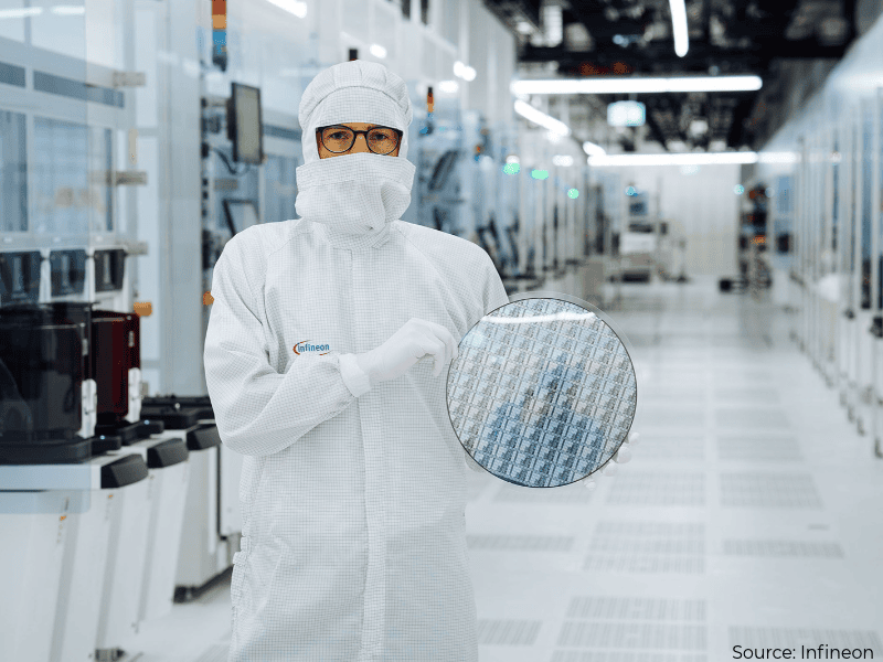
WorldIndustrialWeekly’s General coverage starts from one visible number: €1.1bn. That is the scale of the commitment that Infineon Technologies has put behind a Gallium Nitride (GaN) power-chip project in Villach, Austria, where the company states it is allocating around €1.1 billion to build what it calls the world’s first high-volume GaN power-semiconductor factory on 300mm wafers. The schedule points to manufacturing by the end of 2027, and the spending plan runs through 2034.
Behind the headline figure are several industrial decisions: whether larger wafers can lower unit economics, whether a site already tied to power electronics can convert know-how into capacity, and whether public support under the European Chips Act can remain a bridge while national approval processes continue. The answer will be watched by equipment buyers, automotive supply chains, data-centre operators and energy-systems engineers.
Case snapshot: using Villach’s industrial base to scale GaN
The proposed plant is not being described as an isolated greenfield factory. Infineon says it will make use of cleanroom capacity already present at Villach, then connect it with upgraded production lines. That choice is relevant because it reduces the need to rebuild every element of the manufacturing chain, including facilities, qualification processes and site expertise.
The technical foundation was laid when Infineon processed its first 300mm GaN wafers in 2024. The company reported that the platform can produce approximately 2.3 times as many chips per wafer as conventional 200mm manufacturing. That is a manufacturing economics point before it is a materials point: more usable die on each disk can influence cost, throughput and the speed at which a newer device family reaches mainstream applications.
Jochen Hanebeck, CEO of Infineon Technologies AG, said, “This substantial investment shows our clear commitment to strengthening the European semiconductor ecosystem and Europe’s technological sovereignty. By establishing high-volume manufacturing on 300-millimeter wafers, we will be the first company in the world to bring gallium nitride power electronics into volume production,” in the company’s account of the project.
Relative to silicon-based power devices, GaN parts are associated with faster switching, lower losses and reduced heat generation. Those differences support smaller, more efficient power-conversion designs.
Policy support and workforce context in Europe
The project receives €319 million in state aid approved by the European Commission under the European Chips Act. However, formal funding approval from Austria’s Federal Ministry for Economic Affairs, Energy and Tourism is still pending. For readers evaluating policy-backed industrial expansion, the distinction matters: one part of the support is already cleared, while another stage remains dependent on national procedures.
Policy is only part of the context. The investment is also intended to strengthen semiconductor manufacturing capacity in Europe and to support collaboration among industry, universities, research organizations and smaller technology companies. Villach is described as a major center for power semiconductor research and manufacturing operations, with around 4,800 people employed at the site and approximately 5,800 employees across Austria.
The new facility is expected to link GaN manufacturing more closely with ongoing power-electronics R&D in the region, creating a pathway where design, materials, process and production remain within one industrial cluster.
Data citation: GaN market forecasts and demand drivers
| Metric | Reported figure | Timeframe | Relevance for industrial planners |
|---|---|---|---|
| Possible global GaN power semiconductor market size | approximately $3.5 billion | by 2031 | Shows the commercial space that high-volume 300mm capacity could serve. |
| Expected annual growth | around 35% | between 2025 and 2031 | Highlights why a capacity plan may extend through 2034. |
| Wafer productivity comparison | approximately 2.3 times as many chips per wafer | from the 2024 processing step | Connects 300mm manufacturing with cost and throughput arguments. |
The forecast comes from Yole Group’s Power GaN 2026 report. The report indicates that the global GaN power semiconductor market could reach approximately $3.5 billion by 2031, representing annual growth of around 35% between 2025 and 2031. Demand is expected to accelerate as AI infrastructure, energy systems, e-mobility and robotics require increasingly efficient power conversion.
For Infineon Technologies, moving to 300mm manufacturing provides a route to greater production scale as GaN moves beyond niche applications into mainstream power electronics.
Common mistakes in interpreting the 300mm GaN story
- Reading the project as only a wafer-diameter change. The plan depends on already available cleanroom capacity in Villach, a prior 2024 processing milestone and alignment with demand.
- Treating public support as fully secured. The €319 million from the European Commission under the European Chips Act is approved, but the Federal Ministry for Economic Affairs, Energy and Tourism must still issue formal national funding approval.
- Separating device performance from manufacturing readiness. GaN offers faster switching, lower losses and reduced heat, yet commercial scale still requires high-volume output by the end of 2027 and capacity planning through 2034.
- Ignoring regional industrial assets. The workforce and research ecosystem around Austria’s site, including around 4,800 people and approximately 5,800 employees across Austria, are part of the expansion’s practical base.
Action suggestions for managers, engineers and supply-chain teams
- Validate the timing assumptions. When building a 2027 or 2028 product roadmap, anchor GaN supply expectations to the stated manufacturing start date by the end of 2027, while recognizing that investment continues through 2034.
- Map application fit first. Power electronics teams should compare designs against the reported advantages of GaN: faster switching, lower power losses and reduced heat generation.
- Monitor policy completion. Procurement and investment analysts should track the remaining approval step at the Federal Ministry for Economic Affairs, Energy and Tourism, not just the European Commission decision.
- Read market data alongside capacity plans. If the GaN market approaches approximately $3.5 billion by 2031 and grows around 35% between 2025 and 2031, then a 300mm line is less a lab experiment and more a mainstream supply strategy.
FAQ: key questions for WorldIndustrialWeekly readers
What is Infineon building in Villach?
Infineon Technologies is building what it says will be the world’s first high-volume manufacturing plant for gallium nitride (GaN) power semiconductors on 300mm wafers. The funding commitment is around €1.1 billion, and the wider project is expressed as €1.1bn.
When does production matter?
The stated start date is by the end of 2027. The investment plan runs through 2034, indicating that the project is meant to mature over a multi-year industrial timeline.
Why are 300mm wafers important?
Infineon processed its first 300mm GaN wafers in 2024 and says the approach can yield approximately 2.3 times as many chips per wafer compared with conventional 200mm manufacturing.
What European support is already in place?
The project receives €319 million in state aid approved by the European Commission under the European Chips Act. Formal funding approval from Austria’s Federal Ministry for Economic Affairs, Energy and Tourism is still pending.
How large could the GaN market become?
Yole Group’s Power GaN 2026 report says the global GaN power semiconductor market could reach approximately $3.5 billion by 2031, with annual growth of around 35% between 2025 and 2031.