
WorldIndustrialWeekly General Brief: IBM’s Chitose Presence Strengthens Rapidus’s 2 nm Road to 2027
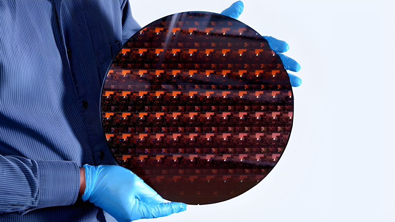
A new chapter in advanced semiconductor manufacturing is taking shape around Chitose, Hokkaido, as IBM deepens collaboration with Rapidus by setting up a presence in the city. For Japan’s industrial ecosystem, the move matters because Chitose is where Rapidus’s first 2 nm wafer plant is being built, with mass production targeted for 2027. The project is positioned to rebuild domestic competitiveness in leading-edge logic and to narrow the distance to TSMC, Samsung Electronics and Intel.
From policy objective to factory reality
Rapidus is a strategically supported semiconductor company backed by the Japanese government. Its backers include Toyota, Denso, Sony Group, SoftBank, NTT, Kioxia, NEC and Mitsubishi UFJ Bank. The company views 2 nm as the lever to restore Japan’s position in advanced chip manufacturing, while Tokyo treats leading-edge logic as an issue of economic competitiveness, industrial security and supply-chain autonomy.
IBM’s role is to transfer and industrialize the 2 nm manufacturing technology it has developed. Rapidus obtained a license for IBM’s 2 nm process technology, and the two parties continue joint research. A local IBM presence in Chitose is expected to strengthen technology transfer, talent development and production readiness for the 2027 target.
Construction of the Chitose plant is progressing. Earlier, the company started installation of equipment related to a trial production line. In the next few months, it plans to expand process verification, creating a bridge toward full-scale 2 nm mass production in 2027.
Case note: a direct jump to 2 nm
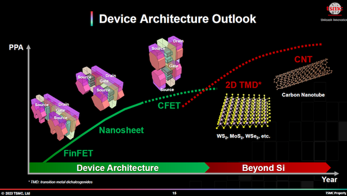
Rapidus is entering the leading-edge logic market by starting directly at the 2 nm node, rather than climbing up from more mature process nodes. In case terms, this is a high-risk, high-reward industrial strategy: if the Chitose facility reaches volume output on schedule, Japan could return to the front of advanced logic manufacturing after decades without top-tier leadership, while global buyers could gain another source of leading-edge supply and reduce reliance on existing main wafer foundry centers.
Data and policy reference points from the announcement
| Reference point | What it signals |
|---|---|
| Chitose, Hokkaido | Physical center for Rapidus’s first 2 nm wafer plant and IBM’s on-site support presence. |
| 2 nm | Leading-edge logic node licensed from IBM and pursued as a shortcut to advanced competitiveness. |
| 2027 | Target year for mass production and the practical test for equipment installation, process verification and yield learning. |
| Japanese government support | Policy alignment around economic competitiveness, industrial security and supply-chain autonomy. |
Common misconceptions
- The partnership is not simply a branding exercise: IBM’s licensed 2 nm technology and ongoing joint research are the operational backbone for Rapidus’s production preparation.
- The Chitose move does not mean volume output is already achieved; plant construction, trial-line equipment installation and expanded process verification remain milestones before 2027.
- Entering at 2 nm is not a linear upgrade from mature nodes; it compresses time but raises technical, manufacturing and supply-chain risk.
Action recommendations for industrial readers
- Track the Chitose milestones: equipment installation, process verification expansion and the stated 2027 mass-production target.
- Monitor Japanese government support and policy framing, because the project is tied to industrial security and supply-chain autonomy, not only commercial manufacturing.
- Evaluate exposure to concentrated advanced-node supply by watching how Rapidus’s 2 nm path could add a new leading-edge source for global customers.
FAQ
Why is IBM located in Chitose?
IBM set up a presence in Chitose to support Rapidus’s first 2 nm wafer plant and strengthen technology transfer, talent development and production readiness.
What does Rapidus hope to achieve by 2027?
Rapidus aims to move from construction and process verification toward 2 nm mass production in 2027.
Why does Japan care?
Tokyo sees advanced logic chips as tied to economic competitiveness, national industrial security and supply-chain autonomy.
Bottom line
For WorldIndustrialWeekly’s general industrial audience, the significance of IBM’s Chitose presence is not that one foreign technology provider has entered Japan, but that a licensed 2 nm platform, a Hokkaido plant, Japanese government backing and a 2027 volume target are being aligned in one project. If Chitose turns verification into production, the impact will extend from factory floors in Hokkaido to global supply-chain decisions about where the most advanced logic chips will come from.