
AI Memory Supply Chain Shift: CXMT Targets HBM3E Mass Production by End of 2026
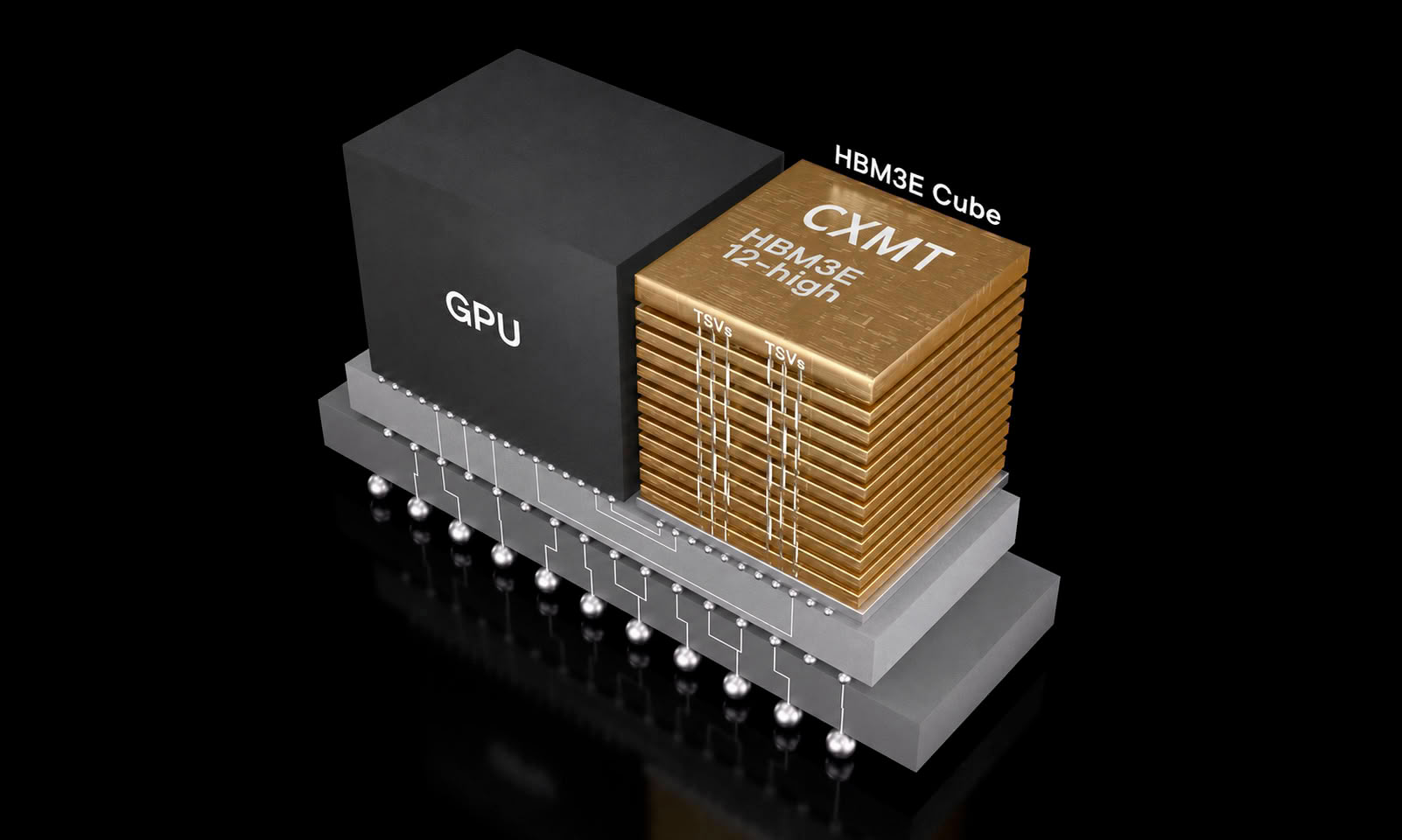
For managers planning accelerator procurement, server refreshes and domestic AI hardware sourcing, the most important signal is not a new memory brand alone; it is a schedule. ChangXin Memory Technologies, also referred to as CXMT, is reported to be preparing to bring HBM3E into the mass-production stage within the next two months, while pointing the formal launch window toward the end of 2026. Because the company started risk trial production and customer sample delivery in August this year, the current task is to turn early hardware validation into a commercial path.
Why HBM3E sits at the center of the AI memory debate
HBM is not an incremental DRAM alternative. In AI accelerators, data-center GPUs and high-performance computing systems, high-bandwidth memory is one of the most critical storage technologies because it moves data fast enough to support training and serving of large AI models. At present, the global HBM market remains mainly controlled by SK Hynix, Samsung Electronics and Micron.
For industrial readers, the technical baseline matters because it shows where a China-based entrant is trying to join the mainstream. According to JEDEC-standard HBM3E, the architecture uses a 1024-bit bus. Per-pin transfer rates may range from 9.2Gbps to 12.4Gbps, and 9.6Gbps is described as a common configuration. The overall bandwidth is about 1.2TB/s, with capacity configurations from 24GB to 36GB. The main stack forms are 8-layer stack and 12-layer stack.
Specification snapshot
| Dimension | Reported HBM3E baseline |
|---|---|
| Bus architecture | 1024-bit |
| Per-pin rate | 9.2Gbps to 12.4Gbps; 9.6Gbps common |
| Aggregate bandwidth | About 1.2TB/s |
| Capacity range | 24GB to 36GB |
| Stack formats | 8-layer stack and 12-layer stack |
Yield, TSV stacking and the production gap
The obstacle is not demand. It is stack yield. HBM3E requires multiple DRAM dies to be connected vertically through through-silicon via (TSV) structures, and both wafer fabrication and packaging complexity become gatekeepers for capacity expansion. Industry information says CXMT's overall HBM3E yield is currently around 20% to 30%, which still leaves a clear distance from internationally leading manufacturers.
The stage-by-stage picture adds nuance. The reported front-end wafer manufacturing yield is about 30%. Once the product enters back-end packaging, the pass rate can improve by about 70%, but the final overall yield still needs further improvement. In practical terms, this means vertical stacking is where early supply constraints are most likely to show up.
The TSV difference that makes stacking difficult
TSV technology maturity is described as the most prominent technical difficulty facing CXMT. Compared with international vendors, there remains a gap in stacking processes. In the HBM2 era, Samsung used about 5000 TSV connections in a single layer. In SK Hynix's HBM3 products, the number has exceeded 8000. CXMT, by contrast, is reported to be trying to achieve HBM3E designs with about 3000 TSV connections. This design direction places higher demands on manufacturing precision and reliability.
Because of these technical conditions, the short-term product focus is expected to be on 8-layer stack HBM3E products, rather than rapidly advancing toward larger-capacity 12-layer stack products.
Samples, testing and what early performance indicates
Reports indicate that CXMT has delivered two versions of HBM3E samples to domestic AI chip companies. One is a standard version; the other is a new version optimized for yield. The samples are now in customer-side testing and validation.
From a performance standpoint, preliminary testing suggests that the current product is closer to SK Hynix's previous-generation HBM3 than to the most advanced international HBM3E products. Market participants still note that, for a vendor entering the HBM field, reaching mass production would itself constitute a major breakthrough.
Case signals already visible in the supply chain
- Factory validation: CXMT began risk trial production in August this year and has already sent customer samples, moving from technology demonstration toward commercial readiness.
- Customer testing: two versions of HBM3E samples are being tested by domestic AI chip developers, including standard and yield-optimized variants.
- System-level pressure: recent AI chip price increases have been widely attributed in part to high-bandwidth memory supply, increasing attention to domestic alternatives.
- Buyer-side interest: Alibaba T-Head and Cambricon were previously reported to have tested domestic HBM solutions in order to reduce reliance on overseas supply chains.
Why domestic AI hardware makers care
Even with current yield limitations, CXMT has incentives to continue toward production. The demand driver is the fast growth of high-bandwidth memory needs among China AI chip manufacturers. Tight advanced AI memory supply and import-restriction pressure have made a domestic HBM source strategically important.
Analysts expect that, if customer validation goes smoothly, domestic AI accelerator products using CXMT HBM3E may enter the market as early as 2027. Compared with global leading vendors, there is still a technology gap of one to two generations. Yet CXMT's entry into HBM means the local AI hardware ecosystem is filling a key missing component and is starting to challenge the high-end AI memory market.
Common misconceptions to avoid
- Sample delivery is not the same as qualified mass production. The reported schedule still depends on customer testing and yield improvement.
- Choosing 8-layer stack first should not be read as abandoning 12-layer stack. The material says the 12-layer route is not expected to advance rapidly in the short term because of technical constraints.
- A 1.2TB/s bandwidth figure does not automatically translate into deployable supply. Yield, packaging and validation are the bottlenecks.
- A lower TSV count is not simply a manufacturing shortcut. It can increase precision and reliability requirements.
Action suggestions for industrial decision makers
- Monitor the two-month production preparation window and the formal end of 2026 milestone, rather than treating the announcement as completed mass production.
- Keep procurement plans tied to verified yield data, especially the reported 20% to 30% overall yield band.
- Distinguish early customer testing from system performance parity: current samples may track SK Hynix's prior HBM3 level rather than leading HBM3E.
- Watch 8-layer stack qualification first, then use it as a leading indicator for whether 12-layer stack expansion becomes realistic later.
Frequently asked questions
Is CXMT already producing HBM3E at commercial volume?
No. It is reported to be preparing to bring HBM3E into the mass-production stage within the next two months, with the formal launch window aimed at the end of 2026. Risk trial production began in August this year.
What is the technical standard being referenced?
JEDEC-standard HBM3E is cited: 1024-bit bus architecture, per-pin rates from 9.2Gbps to 12.4Gbps, common 9.6Gbps, about 1.2TB/s bandwidth, and capacity options from 24GB to 36GB.
What is the biggest near-term constraint?
Yield and TSV stacking. The reported overall yield is around 20% to 30%, while the front-end wafer stage is about 30% and back-end packaging can improve pass rates by about 70%.
How far behind are global leaders?
The gap is described as one to two generations. Preliminary sample performance is closer to SK Hynix's HBM3 than to advanced international HBM3E products.
Bottom line
For China's AI hardware supply chain, CXMT's HBM3E effort is less a product launch than a feasibility test: can a domestic memory maker convert a 20% to 30% yield problem into a repeatable HBM supply source before the end of 2026? If customer validation succeeds and a first 8-layer stack product reaches the market, the 2027 accelerator pipeline would gain a local option. If not, the project will still provide a useful signal about how far the manufacturing ecosystem must travel before high-end AI memory becomes a routine procurement choice.