
WorldIndustrialWeekly General Desk: ChangXin Completes 4F² Engineering Verification As DRAM Scaling Turns Toward 3D
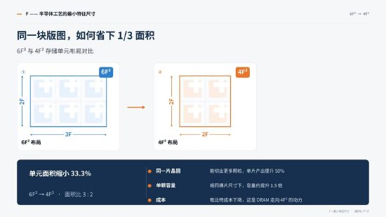
A memory-cell transition is often debated by researchers in terms of area, layout, and device structure, but for industrial operators the more practical question is when a roadmap geometry becomes a verified wafer flow. The reported completion of ChangXin’s 4F² engineering sample verification places the company inside that transition window. The milestone changes the conversation from theoretical scaling to production readiness: which metrics have already reached design expectations, what validation remains before volume supply, and when server-oriented memory products may start to absorb the new cell format.
What engineering sample verification changes for production planning
From a manufacturing practice perspective, the completion of engineering sample verification means that core performance indicators of the platform have reached design expectations on real wafers. That is a meaningful gate, but it is not the final gate. The next checkpoint is customer verification; after that stage is complete, large-scale mass production can be opened. ChangXin has previously said in public presentations that, by year-end, it expects to introduce a new generation of DDR5 RDIMM products integrating advanced 4F² technology for servers, one of the most difficult application fields. For buyers and system teams, this timing turns a device milestone into a product and supply-chain planning milestone.
Global progress read by manufacturers
Publicly disclosed progress shows that ChangXin is at the front of global 4F² engineeringization. Samsung and SK Hynix have both listed 4F² as a key direction for technology below 10nm, while ChangXin completed engineering sample verification ahead of the disclosed peer schedule. If subsequent progress continues smoothly, ChangXin may become the first company in the world to land 4F². The wording is important: the public record points to a lead position in engineering verification, not to an already completed volume transition.
Why the cell shrink is treated as a critical path
The long-term logic of DRAM remains density: fitting more cells on the same wafer area spreads the unit cost of each bit across the manufacturing flow. Once technology enters the 10nm class, the mainstream 6F² layout becomes difficult to sustain because it is approaching physical limits. The IEEE International Roadmap for Devices and Systems (IRDS) states: "the transition from 6F² to 4F² cells is the most promising path to maintain the cost trend." In that framework, 4F² is viewed as the key path for breaking the DRAM scaling bottleneck and moving toward 3D DRAM.
Area, platform choice, and the 3D bridge
By geometry, a 4F² cell occupies 2F×2F, where F refers to the minimum line width or space achievable by lithography. Its area is about two-thirds of the mainstream 6F² cell. That reduction has made 4F² a common direction among major global memory producers. SK Hynix has placed the 4F² vertical gate (VG) platform and 3D DRAM alongside each other as two major technology pillars. Samsung presented a 10nm-class 4F² paper at ISSCC 2026, and its CTO publicly confirmed in October this year that it is also developing the technology. Industry observers also regard 4F² as a necessary stage toward 3D DRAM.
A case view: ChangXin’s VSG and decoupled build
The disclosed ChangXin 4F² architecture is anchored by a self-developed VSG transistor, meaning Vertical Surrounding Gate. Because a vertically surrounding channel structure provides stronger gate control, short-channel effects and leakage can be mitigated. At the architecture level, the approach decouples DRAM manufacturing from CMOS manufacturing, then connects the two through wafer-level hybrid bonding for high-speed interconnect. This separation allows logic performance, memory density, and reliability to be optimized along separate paths rather than forced into a single compromised process window.
How to read the industrial signal without overclaiming
The disclosed milestones can be read as a sequence: design expectation, real wafer confirmation, customer validation, then scale production. The first three steps are technical; the last step is commercial and manufacturing discipline. For this reason, the story is not only about memory cell size. It is about whether the supplier can keep 4F² device behavior stable while entering the verification flow used by customers. The current evidence says the platform has reached a real-wafer design-expectation point, but the downstream validation gate still defines the path to volume availability.
Why server memory is a useful demand-side test case
Server applications are singled out because they are described as one of the most demanding areas. If a DDR5 RDIMM product integrating 4F² technology appears as planned by year-end, the test moves from cell-level behavior to product qualification. That shift matters for industrial readers: a memory platform becomes a supply-chain event when it is designed into a recognizable end product, not only when it appears in a technical presentation or roadmap discussion.
Data and milestone table for industrial readers
| Item | Disclosed value | Why it matters |
|---|---|---|
| Cell area | 2F×2F | Defines the layout advantage over 6F². |
| Area relative to 6F² | About two-thirds | Shows density potential and cost-per-bit pressure relief. |
| Platform status | Engineering sample verified | Indicates core metrics reached design expectations on real wafers. |
| Next gate | Customer verification | Scale production opens only after this stage is complete. |
| Expected product timing | year-end DDR5 RDIMM | Signals a server application entry point for 4F² integration. |
| Roadmap citation | IRDS quote on 6F² to 4F² | Positions the transition as the most promising path for the cost trend. |
Common misconceptions
- Engineering sample verification is not yet customer verification. The milestone proves design expectations on real wafers; mass production still depends on downstream validation.
- 4F² is not merely a shorter name for a smaller cell. It is presented as the structural bridge toward 3D DRAM.
- Company-level progress should not be read as guaranteed mass production. The disclosure says a possible world-first landing depends on smooth follow-on progress.
Limitations of current disclosure
The public facts do not confirm large-scale production. They confirm that engineering sample verification has been completed, that core indicators reached design expectations on real wafers, and that customer verification remains ahead. They also do not remove dependency on subsequent progress. This limitation is not a weakness in the reported milestone; it is simply the normal boundary between engineering proof and commercial manufacturing handover.
Action suggestions
- For memory procurement teams, ask suppliers to define the current stage in the customer verification cycle, not only the existence of an engineering sample.
- For server platform planners, watch the year-end DDR5 RDIMM signal as the first disclosed application window for integrated 4F² technology.
- For process and product engineering groups, review how VSG transistor control and wafer-level hybrid bonding change qualification assumptions for leakage, density, and reliability.
- For strategy teams, treat the IRDS statement about the 6F²-to-4F² transition as a sign that cost trend preservation now depends on cell architecture transition, not only on further lithography spacing shrink.
- For risk owners, separate the three milestones in supplier reporting: wafer verification, customer validation, and volume readiness.
FAQ
Q: What does 4F² mean in this story?
A: It is a DRAM cell layout with 2F×2F area, about two-thirds of the mainstream 6F² cell, and it is viewed as a key path toward 3D DRAM.
Q: Why does the engineering sample verification matter?
A: It means core performance metrics have reached design expectations on real wafers. Customer verification remains the next step before scale production can be opened.
Q: Is ChangXin already the first company to mass-produce 4F²?
A: No. The disclosed report says ChangXin led the engineering sample verification step. If subsequent progress is smooth, it may become the first company in the world to land 4F².
Q: Why do Samsung and SK Hynix appear in the same discussion?
A: Both have publicly linked 4F² to next-generation memory. SK Hynix treats the 4F² VG platform and 3D DRAM as two major technology pillars, while Samsung disclosed a 10nm-class 4F² paper at ISSCC 2026 and confirmed development in October this year.
Q: Does 4F² replace 3D DRAM?
A: No. The source positions 4F² as a path for breaking the DRAM scaling bottleneck and moving toward 3D DRAM, not as the end state.
For industrial decision makers, the practical takeaway is to watch the transition from verified wafer behavior to qualified product availability. The geometry has moved from roadmap language into a production-readiness discussion, but the decisive variables remain customer verification, server product integration, and whether the disclosed early lead converts into the world’s first landed 4F² platform.