
WorldIndustrialWeekly General Analysis: AI Compute Scaling and Panel-Level Packaging, 5 Reasons the Next Decade May Move Beyond Wafers
For production, engineering, and supply-chain readers at WorldIndustrialWeekly, the AI compute question has moved from chip design alone to the packaging line. When accelerators, memory stacks, interposers, and interconnects must work as one system, advanced packaging becomes a scaling constraint and a scaling opportunity. Panel-level processing is now discussed as a practical way to keep that scaling workable for the next decade.
This General column organizes the discussion into five reasons. It is not a vendor comparison and it does not assume a single company can move the industry alone. Instead, it asks a practical question: what does the shift from round wafers to rectangular panels mean for factories, roadmap planning, process qualification, and risk management? The five reasons below connect the technical direction to manufacturing reality, while keeping the analysis anchored to the decade ahead.
Why packaging is now central to AI compute performance
AI systems increasingly depend on tight integration. Processors, high-bandwidth memory (HBM), chiplets, and specialized components must behave as one platform. Advanced packaging affects bandwidth, latency, energy efficiency, and system scalability. In that context, packaging is no longer a back-end support activity; it is part of the performance architecture. That is why more attention is moving to larger formats, and why panel-level packaging is emerging as a possible route for the next decade of AI compute growth.
Five reasons for the momentum
1. Advanced packaging has become the new scaling engine
Current AI accelerators use heterogeneous designs. Multiple chiplets, memory stacks, interposers, and dense interconnect structures are brought together in one package. The value of that integration comes from moving data faster and more efficiently between compute and memory. If packaging progress stalls, silicon scaling alone cannot provide the bandwidth, latency, energy, and performance headroom that large language models and other AI workloads require.
2. Package dimensions are exceeding round-wafer geometry
Advanced packages are growing in size and complexity. Because many packages are square or rectangular, placing them on circular wafers creates a geometry mismatch. Larger rectangular shapes may fit fewer units efficiently across the wafer area, while edge regions become harder to use. As a result, area utilization and manufacturing efficiency become practical constraints. This matters to AI designers because they keep trying to place more compute and memory closer together.
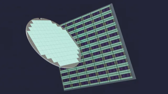 A panel-and-wafer comparison highlights the scaling pressure: AI systems need larger packages, more memory, and faster data movement, while round-wafer layouts run into geometric limits.
3. Rectangular panels can improve area use
Panel-level packaging processes square or rectangular panels rather than conventional round wafers. The larger format can improve area utilization and create opportunities for better manufacturing efficiency as advanced packages continue to grow. The change is not only about substrate shape. It is a broader manufacturing model that may support future package dimensions, improve scalability, and affect production economics. For an industry seeking ways to sustain AI growth, panels are becoming a more attractive route.
4. Panel processing may address future AI bottlenecks
Today, many experts view advanced packaging as one of the most important areas needing investment and innovation. Chipmakers and equipment providers generally try to identify constraints before they throttle growth. Panel-level packaging attracts attention because it addresses a known scaling problem: as AI systems require larger dies, denser interconnects, and more complex package architectures, manufacturing methods must support higher volumes and larger form factors.
The path is not simple. Yield, process control, uniformity, automation, throughput, and standardization remain active development areas. Delivering the precision normally associated with wafer processing on much larger panels will require major engineering innovation. Those difficulties also explain why many observers treat panel processing as an inflection point rather than a minor improvement. If solved, it can open a new era of package scaling beyond wafer-sized constraints.
5. The ecosystem is already building toward the panel future
Large-scale manufacturing shifts historically depend on coordinated work across equipment suppliers, device makers, packaging houses, research groups, and system designers. Panel-level packaging follows that pattern. Progress will depend on new processes, qualified manufacturing flows, better yield, and scalable production models. Advanced packaging has become an ecosystem-driven effort that requires coordination across the semiconductor value chain.
Lam Research has worked on advanced packaging technologies for more than two decades and is investing in infrastructure, R&D capabilities, and ecosystem collaboration for the industry's next chapter. The Salzburg Panel Center of Excellence in Salzburg reflects a broader effort to accelerate panel-level research, qualification, and manufacturing readiness while helping customers prepare for future packaging demands. The effort is not about any single product or platform; it is about enabling the manufacturing foundations future AI systems will require.
Wafer geometry versus panel geometry: a practical comparison
| Planning dimension | Round-wafer packaging | Panel-level packaging |
|---|---|---|
| Substrate shape | Circular wafer surface | Square or rectangular panel surface |
| Fit for large rectangular packages | Geometry mismatch can create edge losses and unused area | Rectangular format can improve area use for rectangular package layouts |
| Scaling pressure | More constrained as package dimensions grow | Potential path for larger package dimensions and denser integration |
| Manufacturing model | Current baseline for many packaging flows | New process model requiring qualification and ecosystem coordination |
| Readiness signal | Established production logic, but facing geometry limits | Developing toward manufacturing readiness for future AI workloads |
Case read: the Salzburg signal for industrial planners
The Salzburg Panel Center of Excellence in Salzburg is best read as a manufacturing-readiness case, not as a finished product announcement. It points to the kind of work required before panel-level packaging can scale: research, process qualification, infrastructure, and ecosystem collaboration. For industrial managers, the lesson is that the transition begins with building qualified capability, not with declaring a new standard.
Data and factual reference points
- Scaling window: the panel route is discussed as a practical path for AI packaging through the next decade.
- Planning horizon: attention is moving to larger formats for the decade ahead.
- Industry status: Today advanced packaging is viewed as a major investment and innovation area.
- Experience reference: Lam Research has been involved in advanced packaging technologies for more than two decades.
- Infrastructure example: the Salzburg Panel Center of Excellence in Salzburg supports research, qualification, and manufacturing readiness.
- Framework reference: the core analysis is structured as 5 Reasons, or five reasons, for momentum.
Common misconceptions
- It is only a bigger substrate. A panel changes layout, process control, and manufacturing economics; it is not just a larger version of the same wafer flow.
- One supplier decides the timeline. The shift depends on equipment, devices, packaging houses, researchers, and system designers working together.
- Yield issues are secondary. Yield, uniformity, automation, throughput, process control, and standardization are central to panel adoption.
- The change is already factory-ready. The transition requires qualification and manufacturing readiness; it is a direction, not an immediate replacement.
Operational implications for manufacturers
For factory planners, panel-level packaging may affect capacity math. Larger rectangular panels can match package geometry more efficiently than round wafers, but the benefit depends on yield and process control. If panel flows improve area utilization and support larger packages, they could reduce the waste created by placing rectangular dies on circular substrates. That has implications for cost per package, tool utilization, and roadmap assumptions.
For engineering leaders, the key question is not simply whether panels exist, but whether qualified flows can deliver performance, reliability, and volume. For supply-chain teams, the likely pattern is staged adoption: existing wafer and packaging lines remain important while panel-level capabilities are developed, tested, and scaled. This creates a hybrid operating environment in which planning, quality, and procurement decisions must tolerate uncertainty.
Risk checklist and action suggestions
- Map current package dimensions against wafer geometry to see where edge loss and layout inefficiency are increasing.
- Track panel-level development signals such as qualification results, yield progress, process-control maturity, automation levels, throughput, and standardization.
- Do not equate investment announcements with immediate production readiness; ask for qualified flows and manufacturing evidence.
- Build supplier and ecosystem engagement early, because the panel future depends on coordinated hardware, process, and qualification work.
- Plan for a gradual transition, not a sudden substitution, especially where AI product roadmaps depend on packaging capacity.
Implementation path: from research to manufacturing readiness
- Process development for panel-compatible packaging formats.
- Qualification of new flows, materials handling, and yield behavior at scale.
- Manufacturing readiness through infrastructure, R&D capability, and ecosystem collaboration.
- Volume transition as production economics, automation, throughput, and standardization mature.
FAQ
Why does AI create packaging pressure?
AI accelerators increasingly integrate processors, high-bandwidth memory, chiplets, and specialized parts. Performance depends on how those parts communicate as one system, which makes advanced packaging a central scaling requirement.
Why do round wafers become limiting?
Large advanced packages are often rectangular. On circular wafers, this can create geometry mismatch, lower usable area, and edge losses, especially as package dimensions increase.
What is the main promise of panel-level packaging?
Rectangular panels can improve area utilization, support larger formats, and create a more scalable manufacturing model for future package dimensions.
What risks remain unresolved?
Yield, process control, uniformity, automation, throughput, and standardization still require development. The transition depends on engineering innovation and ecosystem alignment.
Does this favor one company?
No. The issue is broader than any single product or platform. It concerns the manufacturing foundations that future AI systems may require.
Bottom line
Semiconductor history shows that each major performance era depends on a manufacturing breakthrough. Transistors enabled modern computing. Lithography extended Moore’s Law. Advanced packaging is now helping unlock AI. The next challenge is scaling packaging itself. If AI continues to require larger packages, more memory, and faster data movement, panel-level packaging may become a foundational industrial path for the next decade.