
Gen4 QSiC MOSFETs in 750-V and 1200-V: A Plant-Level Read on 21% Lower On-Resistance and 11% Less Switching Energy
By Michael Torres — WorldIndustrialWeekly Energy desk
For a plant that runs drives, chargers and DC power stages, the useful answer is short: the loss budget inside the cabinet shrinks while the silicon footprint does not. SemiQ's Gen4 QSiC MOSFETs in 750-V and 1200-V classes take on-resistance down 21% and switching energy down 11% against Gen3, on an unchanged 5×5-mm die. Less of the incoming kilowatts become heat, which moves three items plant managers actually track: derating margin, cooling load, and early-life failure rate.
What actually changed in the cell — and what deliberately stayed the same
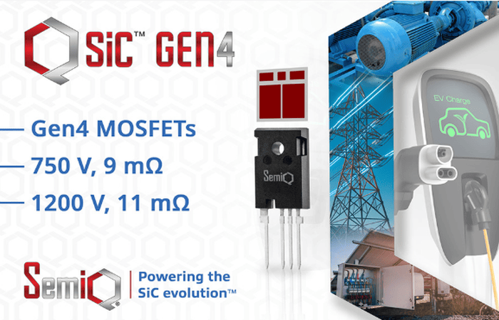
The mechanism is geometry, not a new material story. Gen4 uses an optimized cell topology that reduces cell pitch by 36% compared with previous generations, so more channel area is packed into the same die. Backing that up at the part level: the 750-V GP4T009A075 lands at 9 mΩ and the 1200-V GP4T011A120 at 11 mΩ, the figures SemiQ publishes for the family.
What did not move matters just as much to an operations team. For the 1200-V device the die size remains 5×5-mm — identical to Gen3 1200-V devices — even though total switching energy falls to 1491 µJ. The 750-V SiC MOSFET is a voltage class previous generations never covered, and it posts a total switching energy of just 871 µJ. Same die area, same package, same board outline: this is a spec refresh, not a converter redesign.
| Parameter | 1200-V class, Gen3 reference | Gen4 1200-V GP4T011A120 | Gen4 750-V GP4T009A075 | Why the plant cares |
|---|---|---|---|---|
| On-resistance | Higher by the published 21% delta | 11 mΩ | 9 mΩ | Conduction loss follows I²R, so the saving grows with load squared |
| Total switching energy | Above the Gen4 figure | 1491 µJ | 871 µJ | Multiplies by switching frequency; buys frequency headroom |
| Die area | 5×5-mm | 5×5-mm | Same generation, unchanged layout target | Heatsink path and PCB footprint survive the swap |
| Cell pitch | Previous-generation reference | 36% reduction vs previous generations | Current density per mm² without area growth | |
| Gate-oxide burn-in screening | Not stated | Above 1400 V | Above 800 V | Filters extrinsic early failures before assembly |
| Avalanche test | Not stated | 800 mJ | 800 mJ | Transient energy margin during fault and turn-off events |
| Offer format | — | TO-247-4L (H suffix) or bare die (X suffix) | Kelvin-source driving and discrete parallel design both open | |
| Order status | — | four part numbers, available immediately | No qualification lead time, but also no field history yet | |
How do 21% and 11% translate into watts, kilowatt-hours and cost?
Directly: in modest kilowatt-hours, and in meaningful thermal headroom. Conduction loss is I²R, so a 21% resistance cut removes 21% of that component at a fixed current. Treating the numbers as engineering analysis rather than vendor claims, a switch carrying 25 A RMS dissipates roughly 8.7 W at the back-calculated Gen3 level near 14 mΩ and 6.9 W at the published 11 mΩ — about 1.9 W per device recovered. Across a six-switch three-phase bridge that is on the order of 11 W; across a plant with several hundred in-service drives, the aggregate is a few kilowatts of continuously avoided heat, which for a 500-unit fleet at 8,000 operating hours is a four-figure annual kWh reduction before cooling-fan savings are counted.
Switching energy is where the second number earns its keep. Loss equals energy per switching event multiplied by frequency, so an 11% reduction on a 1491 µJ baseline removes roughly 164 µJ per cycle — about 0.8 W per device at 5 kHz, more at higher frequencies. The strategic reading is not the watt saved but the budget released: lower switching energy lets designers push switching frequency to shrink inductors, transformers and DC-link capacitors, or hold frequency and run cooler. Published comparisons at the conference level report full-SiC conversion stages roughly 3 percentage points more efficient than their IGBT equivalents across the load range, which is consistent with a device-level loss cut of this size.
One correction for anyone building a spreadsheet model: SiC on-resistance has a positive temperature coefficient, so the 9 mΩ and 11 mΩ datasheet values are 25 C anchors. Loss models must use the hot value at the actual junction temperature, and hotter operation partially erodes the conduction advantage — a point documented in industry technical coverage of SiC thermal behaviour.
Why gate-oxide screening and avalanche ratings belong in the uptime file
The screening specification is the least glamorous line in the release and the one most relevant to production continuity. Wafer-level gate-oxide burn-in is applied to the 750-V and 1200-V Gen4 MOSFET dies at voltages above 800 V and 1400 V, respectively, and both are avalanche-tested to 800 mJ.
Reliability research explains why that filter is worth specifying. Work from the Ohio State University SiC power-device reliability group reports that SiC MOS structures show a higher rate of extrinsic gate-oxide failures than silicon MOSFETs, which is precisely why manufacturers implement on-wafer screening or burn-in to strip weak oxides out of the shipped population; a 2025 review in the MDPI journal Electronics makes the same point about early oxide failures appearing in the field. For a maintenance planner, that translates into fewer infant-mortality trips in the first months after a drive rebuild, and a lower probability that one failed switch takes out a whole converter leg and an unscheduled line stoppage.
The avalanche figure works the other way — it is ruggedness against real transients, from bus spikes during fault conditions to energy stored in cabling and busbars. Treat the 800 mJ test result as qualification evidence, not as an operating allowance.
Case reading: a drive refresh that never touched the PCB layout
Consider the pattern most energy managers actually face: an installed base of AC drives and DC/DC stages whose power boards are frozen, with change control that punishes any layout edit. The Gen4 family fits that constraint because the 1200-V die size remains 5×5-mm and the offer format — TO-247-4L or bare die — is unchanged from the previous generation. In our worked example, a 250 kW-class drive stage with twelve paralleled 1200-V switches keeps the same copper, the same heatsink interface and the same mounting hardware; the deliverable change is roughly 23 W of recovered device loss and a cooler junction at the same load, which converts into continuous-current headroom or reduced fan duty rather than an immediate billing line.
The 750-V part opens a different case: battery, energy-storage, DC-bus and onboard-charger power stages that previously had to oversize into a 1200-V switch because no 750-V device existed in the earlier generation. Moving those converters to a purpose-built class typically improves the cost-per-ampere and the loss balance, since the device is no longer carrying voltage capability the bus never uses.
Step-by-step: how to evaluate Gen4 for an existing converter
- Re-run the loss model against the real duty cycle, not the nameplate. Pull hot RDS(on) from the curve at your operating junction temperature and recompute conduction loss with measured RMS current.
- Fix the voltage class first. Audit actual maximum bus voltage plus spike margin; the new 750-V part only makes sense where the DC link genuinely sits in that band, otherwise the 1200-V device remains the correct choice.
- Confirm the driver can exploit the fourth pin. The TO-247-4L package carries a Kelvin source; the driver return must connect to that pin, not be strapped to the power source, and negative turn-off bias should follow the datasheet to hold the device off against fast transients.
- Re-check the commutation loop. Faster switching exposes stray inductance; measure turn-off voltage spike on the board with double-pulse testing before trusting the 800 mJ avalanche rating as headroom.
- Re-derive the thermal case. Same die area means the thermal path is unchanged, so recovered loss becomes either higher continuous current at the same case temperature or smaller cooling demand at the same current.
- Write the screening data into the purchase specification. Require the wafer-level burn-in condition and avalanche test evidence per lot, and keep a second qualified source — a freshly released device has availability, not field history.
Five misconceptions that cost plants money
- "A 21% device improvement is a 21% efficiency improvement." It is a 21% cut in one loss component. Converter efficiency moves in the tenths of a percent; the real prize is thermal margin and power density.
- "Lower on-resistance means I can drop the heatsink." Only after re-deriving the model at hot resistance and worst-case duty; SiC losses move with junction temperature.
- "It is a drop-in, so no testing is needed." Identical die area is not identical behaviour. Gate oscillation, loop inductance and EMI all shift when switching energy and current capability change.
- "Avalanche-rated to 800 mJ, so spikes are free." Ruggedness is a safety net for rare events, repeated avalanche stress still degrades a device; design the snubber and turn-off delays as if the rating were not there.
- "Screening is a vendor quality detail." It is an uptime parameter. Gate-oxide infant failures are the classic early-in-life SiC failure mode, and burn-in data is procurement's only visibility into it.
What this launch signals for industrial energy conversion to 2031
Trend judgment, in three lines. First, device-level efficiency gains are now coming from cell geometry and screening discipline rather than from exotic materials — exactly the kind of increment that industrial retrofits can bank without redesigning equipment. Second, the pull is broadening beyond traction: Yole Group's Power SiC 2026 study sizes the power SiC device market at roughly $11 billion by 2031 on a 20% CAGR from 2025, crediting the 200 mm ramp-up and fast-growing non-automotive demand, including data-centre power stages. Third, the denominator justifies the attention: UNIDO's assessment of electric motor systems puts them at about 60% of global industrial electricity consumption and close to 70% of industrial electricity demand, so any technology that reduces conversion loss inside motor drives, chargers and DC distribution compounds across the whole factory floor.
For energy managers, the near-term consequence is procedural. As more SiC part numbers reach the field, the questions that separate good specifications from marketing sheets become verifiable ones: what burn-in voltage was applied to the lot, at what statistics, and what avalanche and short-circuit evidence ships with it.
Action recommendations for the Energy desk
- Add gate-oxide screening conditions (above 800 V for the 750-V class, above 1400 V for the 1200-V class) and 800 mJ avalanche evidence to your standard power-semiconductor purchase specification.
- Inventory the converters in service by DC-bus voltage, and flag those running 500–600 V buses that have been over-rated at 1200-V devices; the new 750-V class is where the cost and loss case is easiest to defend.
- Ask your drive OEM whether the Gen4 refresh can be taken on existing boards, given the unchanged 5×5-mm die and package — a yes turns an efficiency project into a spare-parts upgrade with no layout change control.
- Model savings as cooling load and derating margin, not only as kWh: the fan duty and cabinet air-conditioning side of the ledger often outweighs the device loss itself.
- Qualify two sources before committing a fleet; immediate availability of the four part numbers today is not a supply guarantee for a multi-year retrofit program.
FAQ: what plant engineers ask first
Which part numbers should I be quoting?
All four are available immediately: GP4T009A075H and GP4T009A075X for the 750-V device, GP4T011A120H and GP4T011A120X for the 1200-V device. The H suffix denotes the TO-247-4L package and the X suffix denotes bare die.
Is the 11% switching-energy saving worth changing frequency?
Only if the board can absorb faster edges. Switching loss scales linearly with frequency, so the 11% cut gives headroom, but stray inductance, driver peak current and EMI limits decide whether you actually spend it.
What applications does SemiQ target with this family?
EV chargers, solar inverters, industrial drives, and high-voltage DC/DC and DC/AC converters — the same classes that dominate electrical-room and production-line conversion losses.
Should a maintenance department care about burn-in?
Yes. Gate-oxide early failures are the dominant infant-mortality mechanism reported for commercial SiC devices, and wafer-level screening at voltages above 800 V and 1400 V is how the weak population is removed before it reaches your drives.
References
- Yole Group, Power SiC 2026 — Markets and Applications — https://www.yolegroup.com/product/report/power-sic-2026---markets-and-applications/
- UNIDO, Energy efficiency in electric motor systems — https://www.unido.org/publications/ot/9655042/pdf
- Ohio State University SiC Power Devices Reliability Lab, Effects of Oxide Electric Field Stress on the Gate Oxide Reliability of Commercial SiC Power MOSFETs — https://u.osu.edu/sicpowerdevicesreliabilitylab/files/2023/03/Effects_of_Oxide_Electric_Field_Stress_on_the_Gate_Oxide_Reliability_of_Commercial_SiC_Power_MOSFETs.pdf
- MDPI Electronics, Investigation of the Effect of Gate Oxide Screening with SiC MOSFETs (2025) — https://www.mdpi.com/2079-9292/14/7/1366
- ROHM TechWeb, Benefits of a Driver Source Terminal: Comparisons Using TO-247-4L and TO-247-3L — https://techweb.rohm.com/product/power-device/sic/10992/
- EE Power, Understanding the Thermal Behavior of SiC — https://eepower.com/technical-articles/understanding-the-thermal-behavior-of-sic/
- IEEE Power Electronics Semiconductor Applications (PSMA) conference material, How SiC MOSFETs Enhance Efficiency, Reliability and Performance — https://www.psma.com/sites/default/files/IS16.1%20How%20SiC%20MOSFETs%20Enhance%20Efficiency,%20Reliability,%20and%20Performance%20of%20Electric%20Vehicles_0.pdf
Story tips, device data and energy-management case requests: WorldIndustrialWeekly Energy desk at news@industrialweekly.com.